
Enhancing Semiconductor Yield with Automated Lithography Simulation Workflows
How automated lithography simulations with Hyperlith™ and its Python API deliver aerial images, critical dimensions, Bossung plots, process windows and NILS for maximum semiconductor yield.
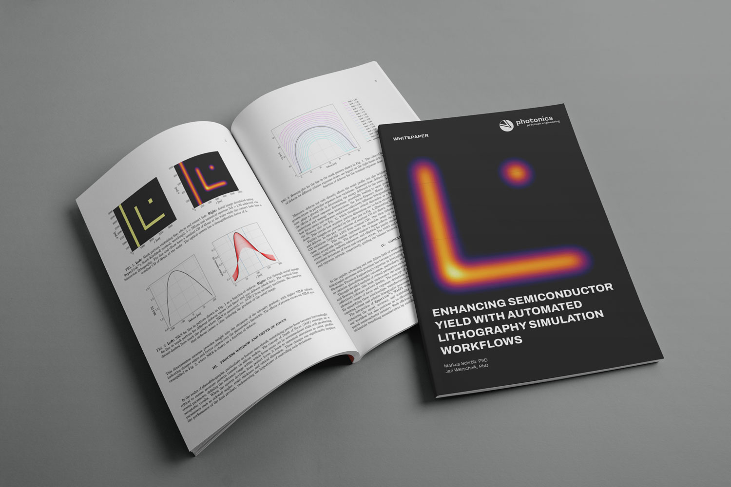

About the white paper
In the rapidly evolving field of semiconductor manufacturing, precise and efficient lithography simulations are crucial for achieving maximum production yield. This white paper demonstrates our expertise in conducting lithography simulations, focusing on key quantities such as aerial images, critical dimensions, Bossung plots, process windows, and Normalized Image Log-Slope (NILS). By leveraging commercial lithography simulation software and automating its processes via API integration, we showcase our ability to deliver accurate and actionable insights. Each quantity is defined and illustrated with figures generated by our simulations, highlighting their relevance in modern semiconductor development. This paper underscores our commitment to innovation and precision in the field of lithography.
Introduction
In the semiconductor industry, lithography stands as a cornerstone of modern chip manufacturing, enabling the transfer of intricate patterns onto silicon wafers with nanoscale precision. As feature sizes shrink and design complexities increase, the need for accurate and efficient lithography simulations has never been greater. At Photonics Precision Engineering, we use Hyperlith™ and its Python API to optimize lithographic processes, ensuring that our clients achieve the highest standards of performance and reliability. This white paper highlights our capabilities in simulating critical lithographic quantities — such as aerial images, critical dimensions, Bossung plots, process windows, and NILS — all facilitated by Hyperlith™’s advanced simulation tools. We demonstrate how automation via Hyperlith™’s Python API enhances the speed, accuracy, and scalability of these simulations, providing a robust framework for meeting the demands of cutting-edge semiconductor manufacturing.
More on lithography imaging


Get the white paper
Fill out the form and your PDF download will be available immediately.